Lab Experiment 7: High-Resolution Gamma-Ray Spectroscopy with HPGe Detectors
Purpose:
- To demonstrate the measurement of gamma-ray energies with high resolution provided by a High-purity Germanium (HPGe) detector.
- To understand the performance differences between counting with a high-resolution system (HPGe) and a low-resolution system (NaI).
Equipment Required:
Theoretical Overview:
Semiconductor detectors
The use of semiconductor detectors for gamma-ray detection has provided tremendous gains in measurement capability. The gamma-ray peaks obtained with NaI detectors are very broad by comparison, so that two peaks close to each other cannot be resolved and low-energy peaks may not be easily observed. Semiconductor detectors made of germanium or silicon compensated with lithium provide significantly better energy resolution.
For semiconductor detectors the thickness of the depletion region (depletion depth) d is given by the following equation:
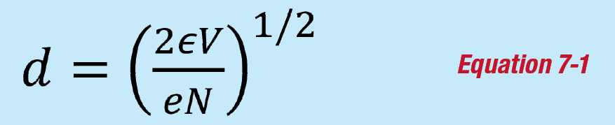
where:
ε is the dielectric constant.
V is the reverse bias voltage.
N is the net impurity concentration in the semiconductor material.
e is the electron charge.
For gamma-ray spectroscopy a large depletion region is required for complete charge collection and increased efficiency. Here for a given reverse bias voltage, the value of N needs to be reduced as much as possible. The high-purity germanium detectors that are being manufactured today can achieve net impurity concentration as low as 0.8 x 1010cm-3.
In insulators, the band gap between the valence band (fully occupied) and conduction band (completely empty) is high, and no electric field or temperature rise can provide enough energy for electrons in the valence band to cross the gap and reach the conduction band (Figure 7-1). However, in semiconductors the band gap is small, and increased temperature, incident charged particles, or applied electric field can impart enough energy to electrons to move them from the valence band to the conduction band. When an electron moves from the valence band to the conduction band, a hole is created in its place in the valence band. Holes behave like particles with positive charge, and they contribute to the overall conductivity of the semiconductor.

Figure 7-1: Band structure in insulators and semiconductors. Eg is the band gap energy.
High-purity Germanium (HPGe) detectors
Germanium detectors are semiconductor diodes having a p-i-n structure (P-type contact, intrinsic layer, and N-type contact), in which the intrinsic (i) region is sensitive to ionizing radiation, particularly X-rays and gamma rays. Under reverse bias, an electric field extends across the intrinsic or depleted region. When photons interact with the material within the depleted volume of a detector, charge carriers (holes and electrons) are produced and are swept by the electric field to the p and n electrodes. This charge, which is in proportion to the energy deposited in the detector by the incoming photon, is converted into a voltage pulse by an integral charge-sensitive preamplifier. For a coaxial detector (Figure 7-2) the rectifying contact that forms the semiconductor junction is typically placed at the outer surface of the crystal. Thus, the outer contact for an n-type HPGe will be p+ and the inner surface will be n+. The depletion layer for such a detector grows inwards as the voltage is increased.
Since Germanium has a relatively low band gap, these detectors must be cooled in order to reduce the thermal generation of charge carriers (thus reverse leakage current) to an acceptable level. Otherwise, leakage-current-induced noise destroys the energy resolution of the detector. Liquid nitrogen, which has a temperature of 77K, has traditionally been the cooling medium for such detectors. Many modern detectors are supplied with an electrical cooling system, thus removing the need for liquid nitrogen. There are two disadvantages with semiconductor detectors. First, high-purity or lithium-compensated crystals cannot be made as large as NaI, so it is not possible to make detectors with the same efficiency. Second, the semiconductor detector must be cooled to near-liquid-nitrogen temperature when in use which adds to the cost and complexity of the system.
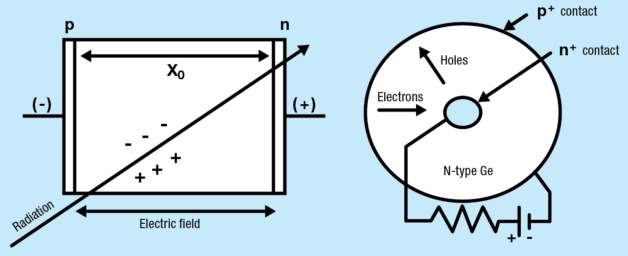
Figure 7-2: A typical p-i-n junction detector (left) with reverse bias. A cross section of an n-type coaxial detector perpendicular to the cylindrical axis (right).
Energy resolution
The energy resolution of a germanium detector can be described as:

where:
wd is the peak width due to detector effects.
we is the peak width due to electronics effects.
The width wd is energy dependent and is given by:

where:
F is the fano factor.
w is the energy required to produce an electron-hole pair.
In case of germanium w (≈3 eV) is low and thus a large number of electron-hole pairs are produced which results in good statistics from the charge collection and therefore a good energy resolution.
The width we is dependent on both the detector capacitance, which in turn depends on the size of the detector, and the bias voltage. Overall the resolution improves with decreasing capacitance.
In a typical broad-energy detector (BE2825) the resolution is 0.4 keV and 2.0 keV at 5.9 keV and 1332 keV, respectively.
Experiment 7 Guide:
Resolution comparison
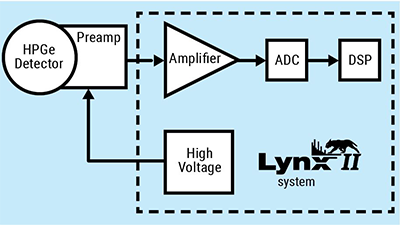
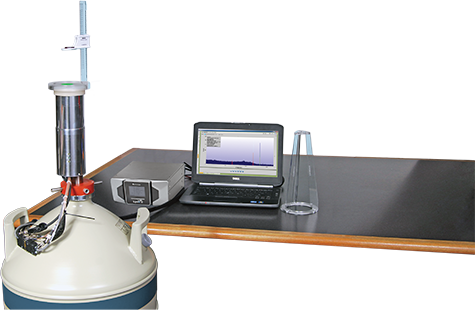
Figure 7-3: Setup for HPGe detector.
1. Ensure that the HPGe detector is connected (via the Lynx II DSA) to the measurement PC either directly or via your local network.
2. Place the 137Cs source in front of the detector.
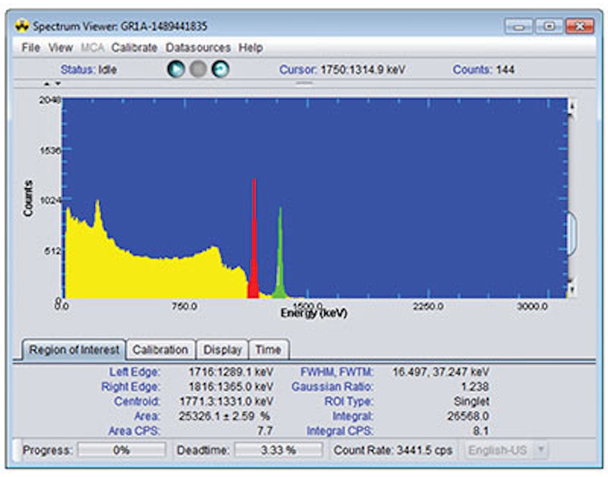
3. Open the ProSpect Gamma Spectroscopy Software and connect to the HPGe detector.
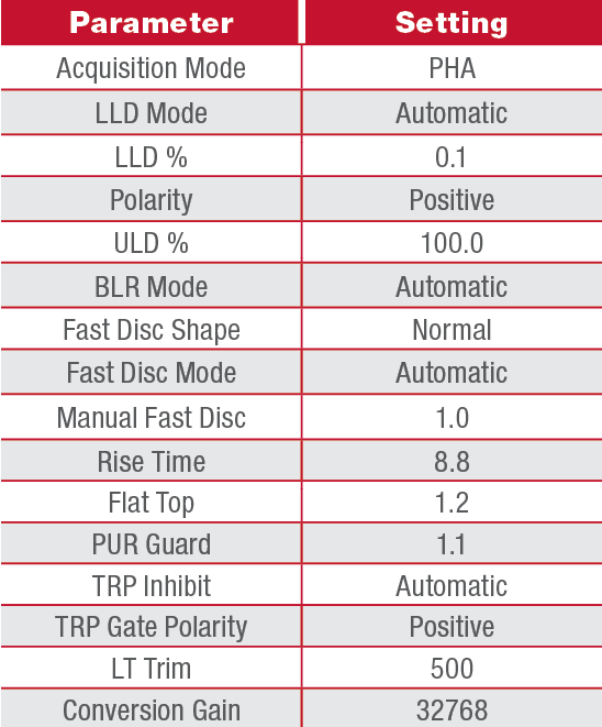
4. Configure the MCA settings as listed in Table 7-1.
5. Use the software to apply the recommended detector bias to the HPGe detector. This can be found on the detector specification sheet or listed on the side of the detector itself.
6. Set the amplifier gain such that the full-energy peak is at 40% of the range of the spectrum.
7. Acquire a spectrum (use a count time such that there is at least 10 000 counts in the full-energy peak).
8. Adjust the energy calibration such that the photopeak is at an energy of close to 662 keV.
9. For the 137Cs photopeak record/determine:
a. Centroid channel and energy
b. ROI range (both channel and energy)
c. FWHM
d. Peak Areas (including the net area, net area uncertainty, and total area)
e. Resolution (calculated in % by taking the FWHM in keV * 100 / centroid in keV)
10. Load the 137Cs spectrum from Experiment 1, obtained using a NaI detector. On the preference tab choose to compare it to the spectrum acquired in step 7. Compare the FWHM values for the full-energy peaks from both spectra.
11. Position the 60Co source and collect a spectrum with the 1173 keV peak and the 1332 peak, the two largest peaks, such that they are in the upper third of the spectrum.
12. Calibrate the energy of the spectrum using the 1173 and 1332 keV peaks.
13. Record the FWHM of the 1332 keV peak in keV. Compare this value against the detector specification sheet, if available. The resolution of germanium detectors is often specified at 1332 keV for high energy applications.
14. Position the 57Co source and collect a spectrum. Observe a peak at 121 keV.
15. Record the FWHM of the 121 keV peak in keV. Compare this value against the detector specification sheet, if available. The resolution of germanium detectors is often specified at this energy for low- to medium-energy applications.
Table 7-1: Standard Gain and Filter Settings for HPGe with Lynx II DSA.