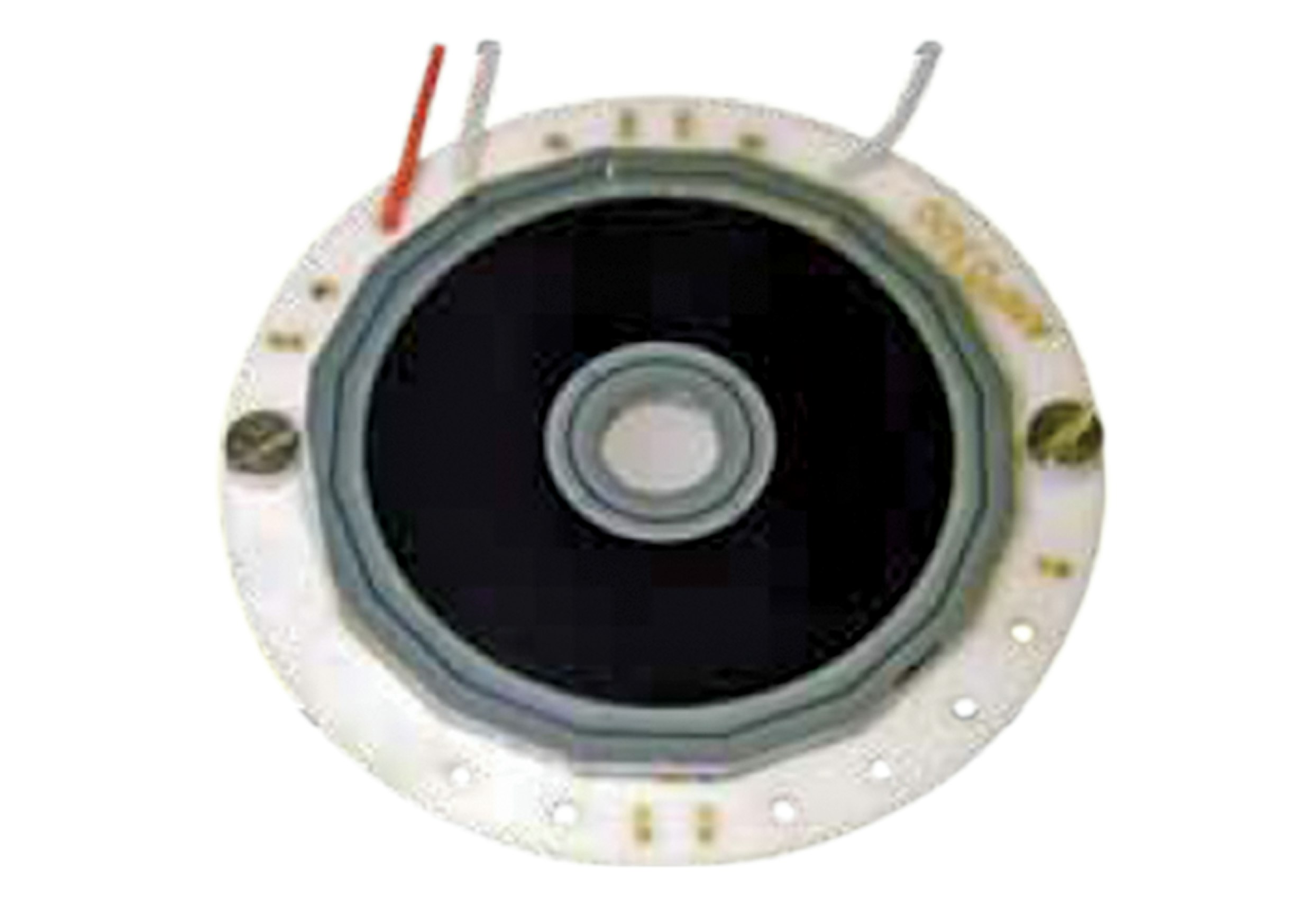
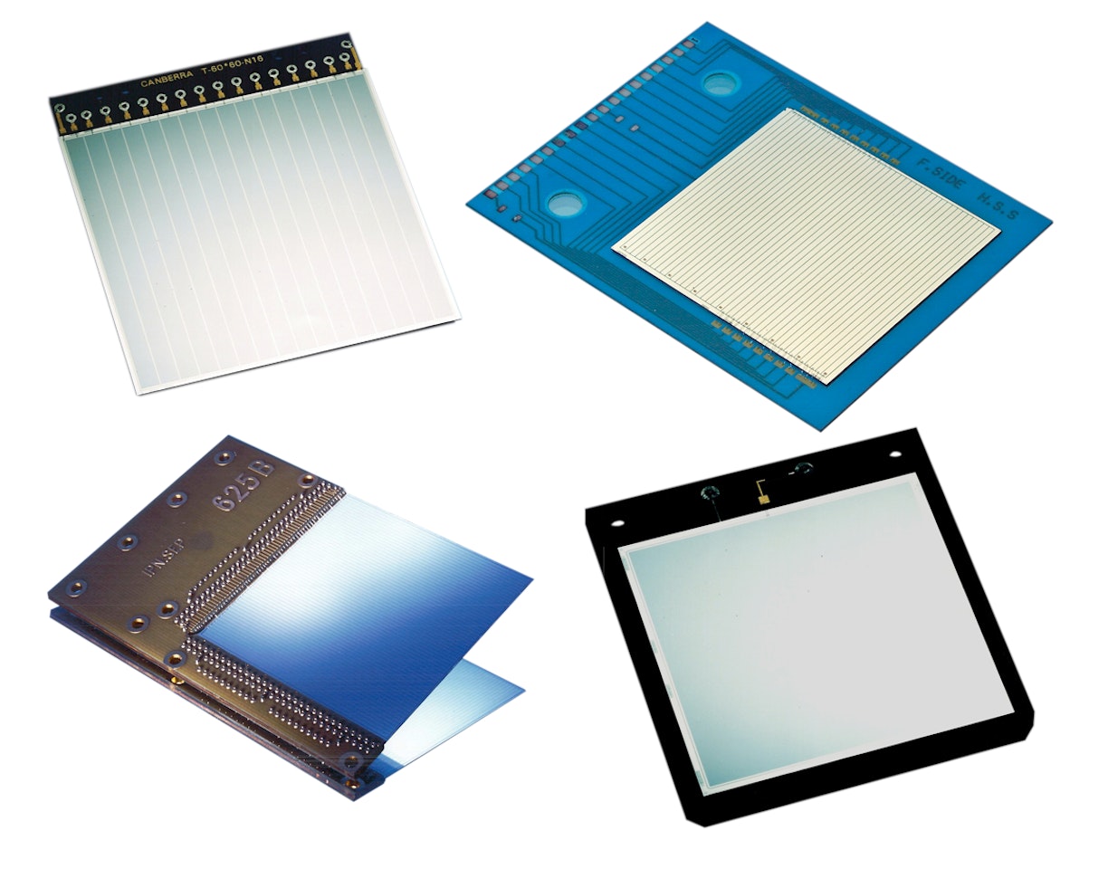
Logo Basic

Photo-diodes

for Synchrotron Applications

Single or multiple junction on ceramic board Electron Beam Detector Si Photodiodes.

Tag Features

  • Single or multiple junction on ceramic board
  • Thin junction entrance window: < 50 nm
  • Low dark current, typically below 1 nA /cm2
  • Active area: 50 to 550 mm2, different shapes or custom design request are possible
  • Diameter hole in center: standard 4 mm, sleeve: 16x3 mm
  • No optical window

Description

Advantages

  • Fast read-out (from ns to ps (FWHM))
  • Used in photovoltaic or biased mode


Applications

  • Direct detection of low energy (>1 keV) electron beams with high sensitivity
  • Backscattered electron for scanning electron microscope (SEM)
  • Photo diodes for synchrotron applications
  • Electron Micro Probe analysis for non-destructive chemical analysis

Do you have a question or need a custom solution? We're here to help guide your research.

Related Products