System Selection Guide
Mirion offers guidance with selections to meet your needs, based on application, software and hardware.
Mirion offers guidance with selections to meet your needs, based on application, software and hardware.
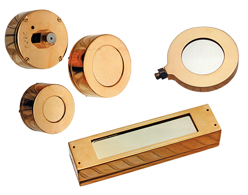
PIPS® (Passivated Implanted Planar Silicon) detectors
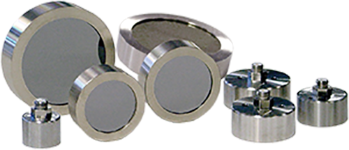
Mirion offers two types of silicon charged particle detectors to cover a wide range of applications. The first type is the PIPS (Passivated Implanted Planar Silicon) detector, which employs an implanted barrier contact that forms a precise, thin, abrupt junction for good charged particle resolution. The second type is the Lithium-drifted silicon detector to address the need for better detection efficiency for high energy charged particles. In both cases, the detectors have a P-I-N structure in which a depletion region is formed by applying reverse bias, with the resultant electric field collecting the electron-hole pairs produced by an incident charged particle. The resistivity of the silicon must be high enough to allow a large enough depletion region at moderate bias voltages.
At the implanted barrier contact junction there is a repulsion of majority carriers (electrons in the n-type and holes in p-type) so that a depleted region exists. An applied reverse bias widens this depleted region which is the sensitive detector volume, and can be extended to the limit of breakdown voltage. PIPS detectors are generally available with depletion depths of 100 to 1000 µm.
These detectors can be used with the Model 2003BT preamplifier. They are also compatible with the Alpha Analyst™ or Model 7401 Alpha spectrometers for sizes up to 1200 mm2.
Detectors are specified in terms of surface area and alpha or beta particle resolution as well as depletion depth. The resolution depends largely upon detector size, being best for small area detectors. Alpha resolution of 12 to 35 keV and beta resolutions of 6 to 30 keV are typical. Areas of 25 to 5000 mm2 are available as standard, with larger detectors available in various geometries for custom applications. Additionally, PIPS detectors are available fully depleted, so that a dE/dx energy loss measurement can be made by stacking detectors on axis. Detectors for this application are supplied in a transmission mount, (i.e. with the bias connector on the side of the detector).
With standard thicknesses between 2 to 5 mm and on request up to 10 mm, these so called Si(Li) detectors have better stopping power than PIPS detectors, addressing the need for better detection efficiency for high energy charged particles. Si(Li) detectors are available in circular geometry between 200 and 500 mm2 and in rectangular shapes, with a resolution starting from 30 keV depending on the size. These detectors are also available in transmission mount.
In case any charged particle localization is needed Mirion can offer segmented Si(Li)’s (see information for LTS Si(Li) type detectors). Si(Li) detectors at room temperature have a large leakage current. To polarize the Si(Li) detectors the voltage drop within the biasing circuits should be minimized. In this frame the resistors within the HV filter or at the AC coupling network should be kept at 10 Mohms value. Mirion recommends 2003BT or 2004 type preamplifiers, but for Si(Li) detectors the resistors in the HV filter and in the AC coupling network should be dropped from 100 Mohms to 10 Mohms to avoid excessive voltage drop.
Lithium drifted silicon detectors
Comparison of PIPS to Lithium drifted silicon detectors
SILICON CHARGED PARTICLE DETECTORS
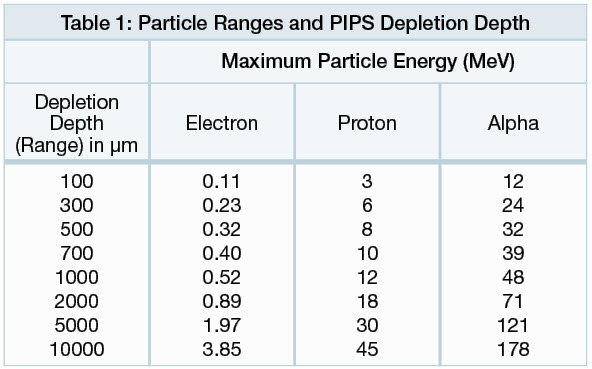
A chart of the energies of various particles measured at several depletion depths is shown in Table 1. Note that even the thinnest detector is adequate for alpha particles from radioactive sources, but that only very low energy electrons are fully absorbed. However, for a detector viewing a source of electron lines, such as conversion electron lines, sharp peaks will be observed since some electron path lengths will lie fully in depleted the region. Figure 1 shows ranges of particles commonly occurring in nuclear reactions.
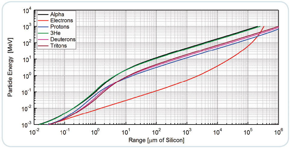
Figure 1 - Range-Energy Curves in Silicon
Since the charge collected from the particle ionization is so small that it is impractical to use the resultant pulses without intermediate amplification, a charge-sensitive preamplifier is used to initially prepare the signal.
Figure 2 illustrates the electronics used in a single-input alpha spectroscopy application. Note that the sample and detector are located inside a vacuum chamber so that the energy loss in air is not involved.
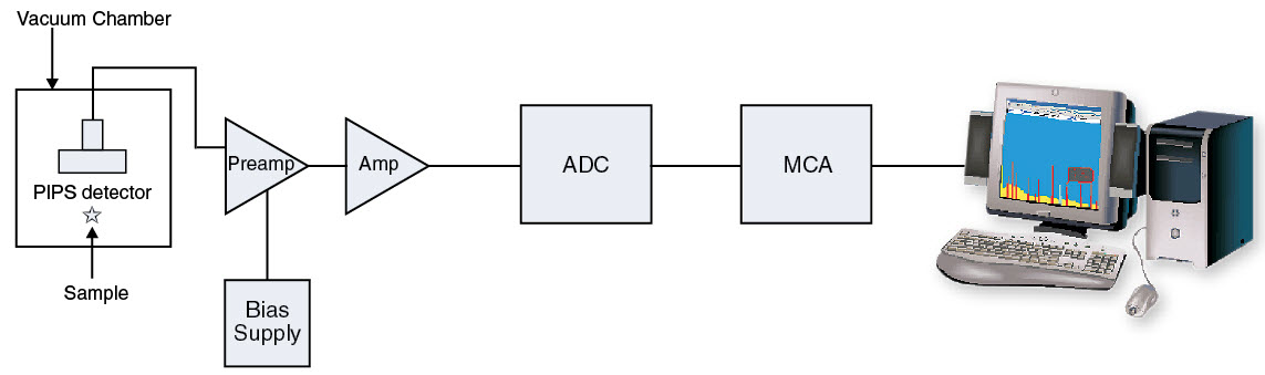
Figure 2 - Electronic chain used in alpha spectrometry
The energy range of the different silicon charged particle detectors is shown in Figure 3, Figure 4 and Figure 5 for energy measurements. The energy range will extend with transmission mounts (FD-series for PIPS and LTC/LTR series for Si(Li)) as detectors can be stacked and used in particle identification, detector telescopes and in other dE/dx measurements.
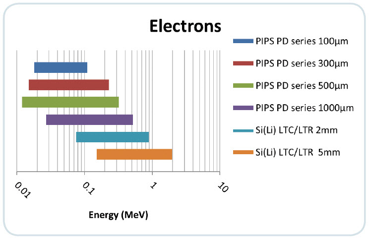
Figure 3 - Energy range of the different detector models for a complete charge collection of electrons
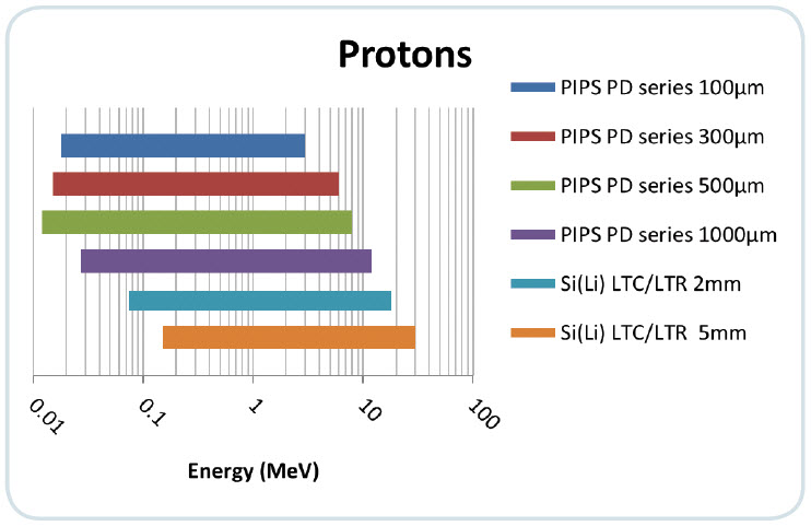
Figure 4 - Energy range of the different detector models for a complete charge collection of protons
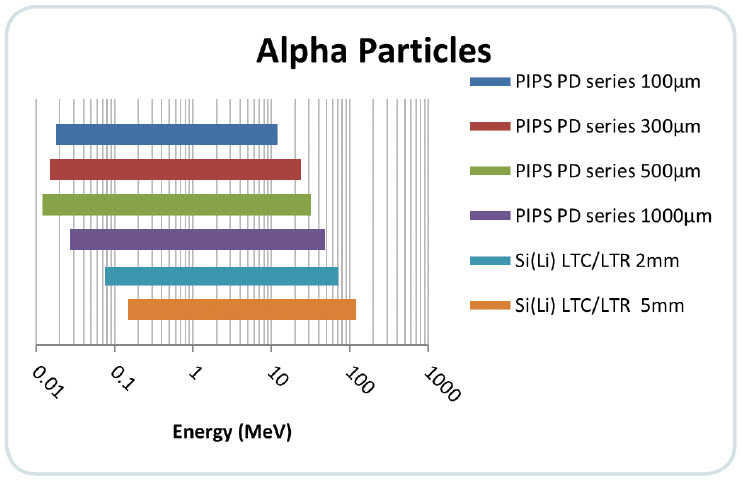
Figure 5 - Energy range of the different detector models for a complete charge collection of alphas
Channeling effects, where energetic ions enter the detector at certain angles will cause channeling of ions between the crystal planes. This effect can cause significant variation of the presented ranges.
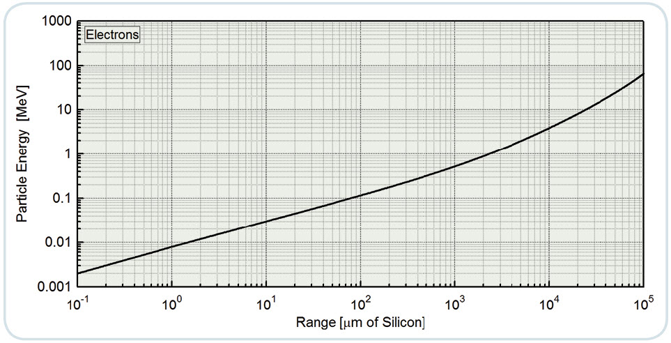
Figure 6 - Energy range for electrons in silicon
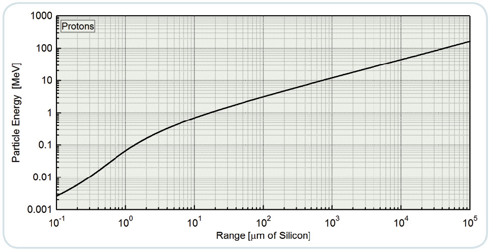
Figure 7 - Energy range for protons in Silicon
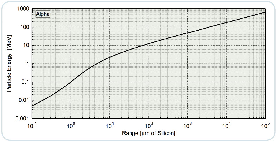
Figure 8 - Energy range for alpha in silicon
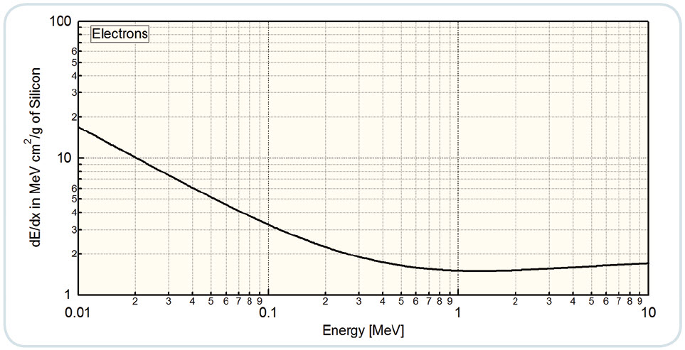
Figure 9 - Energy loss of electron in silicon
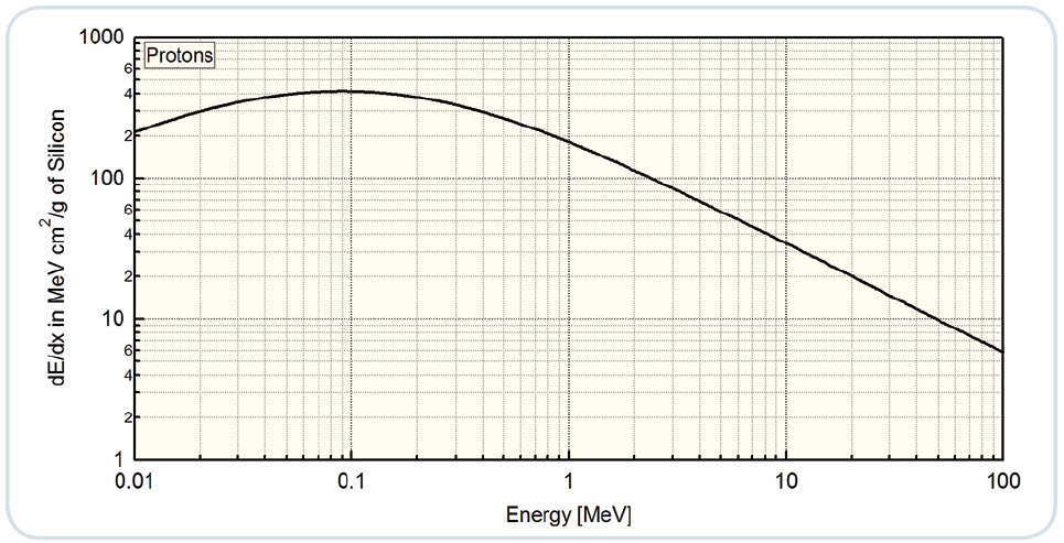
Figure 10 - Energy loss of protons in silicon
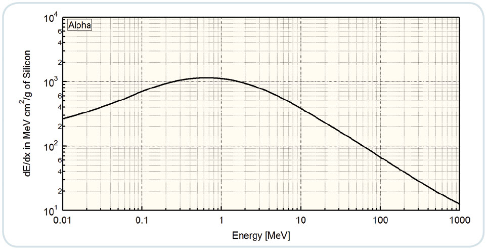
Figure 11 - Energy loss of alpha in silicon
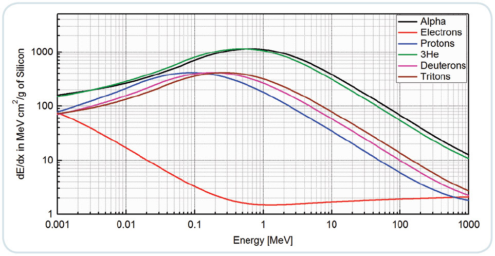
Figure 12 - Energy loss of different charged particles in silicon
Looking for Services or Support?
We're here to help.